Chemical Vapor Deposition (CVD) is a versatile and widely used technique in the field of coating and surface engineering. This process involves the deposition of thin films onto various substrates through the chemical reaction of gaseous precursors. With its ability to precisely control film thickness, composition, and morphology, CVD offers numerous applications ranging from protective coatings to semiconductor device fabrication. In this article, we will explore the intricacies of CVD and highlight its diverse applications in different industries.
Understanding the CVD Process
CVD operates under controlled conditions of temperature, pressure, and gas flow to enable the growth of thin films on solid surfaces. The process typically involves four main steps: precursor delivery, adsorption, chemical reaction, and film formation.
Precursor Delivery
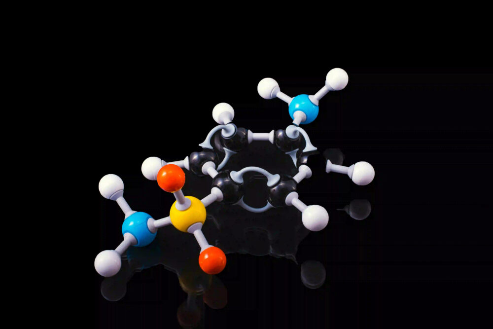
Precursors, usually in the form of volatile liquids or gases, are introduced into a reaction chamber. These precursors contain the desired elements needed for film deposition. For example, in the deposition of silicon dioxide (SiO2), precursors like silane (SiH4) and oxygen (O2) are commonly used.
Adsorption
Once inside the reaction chamber, the precursors adsorb onto the substrate surface. This adsorption can occur through physical or chemical interactions, depending on the nature of the precursors and substrate. The adsorbed precursors then react to form solid-state compounds.
Chemical Reaction
The adsorbed precursors undergo chemical reactions to form the desired film. This reaction is typically initiated by thermal energy or by the introduction of a catalyst. The choice of reaction conditions determines the film’s composition, crystallinity, and microstructure.
Film Formation
As the reaction progresses, the solid-state compounds continue to grow, forming a continuous and conformal film on the substrate surface. The film’s growth rate is influenced by factors such as temperature, precursor concentration, and reaction time.
Applications of CVD in Coating and Surface Engineering
Protective Coatings: CVD is widely employed to create protective coatings with enhanced properties such as hardness, wear resistance, and corrosion resistance. For example, titanium nitride (TiN) coatings are commonly used in cutting tools and wear-resistant components, while diamond-like carbon (DLC) coatings find applications in automotive and aerospace industries due to their low friction and high hardness.
Optical Coatings: CVD plays a crucial role in the production of optical coatings used in lenses, mirrors, and other optical devices. By depositing thin films of materials with specific refractive indices, CVD allows for the manipulation of light transmission, reflection, and absorption. Anti-reflective coatings, high-reflectivity mirrors, and color filters are some examples of optical coatings produced using CVD techniques.
Semiconductor Device Fabrication: CVD is extensively utilized in the manufacturing of semiconductor devices such as integrated circuits and thin-film transistors. It enables the deposition of various materials, including silicon dioxide (SiO2), silicon nitride (Si3N4), and metal films, essential for insulating, passivating, and interconnecting electronic components. CVD also plays a vital role in the growth of epitaxial layers, enabling the creation of high-quality crystalline structures in semiconductor devices.
Chemical Sensors and Catalysts: CVD is employed to create thin films of catalytically active materials used in chemical sensors and catalysts. These films provide high surface area and controlled surface chemistry, which enhance the performance and selectivity of these devices. Gas sensors, biosensors, and heterogeneous catalysts are some examples where CVD-deposited films enable efficient and selective chemical reactions.
Energy Storage and Conversion: CVD is utilized in the production of materials for energy storage and conversion devices. Thin films of lithium cobalt oxide (LiCoO2) and lithium iron phosphate (LiFePO4) are deposited on electrodes for rechargeable lithium-ion batteries. CVD is also employed to create thin films of materials used in solar cells, fuel cells, and supercapacitors, allowing for efficient energy generation and storage.
MEMS and NEMS Devices: Microelectromechanical systems (MEMS) and nanoelectromechanical systems (NEMS) rely on CVD for the deposition of functional materials. CVD allows for the creation of thin films with precise dimensions and tailored properties, enabling the fabrication of microsensors, actuators, resonators, and other miniaturized devices.
Conclusion
Chemical Vapor Deposition (CVD) is a powerful technique that enables the deposition of thin films with exceptional control over their properties. From protective coatings to semiconductor device fabrication, CVD finds applications in numerous industries, contributing to advancements in technology and engineering. Understanding the intricacies of the CVD process and its diverse applications allows researchers and engineers to harness its potential for developing innovative solutions in coating and surface engineering. As technology continues to evolve, CVD will undoubtedly remain a valuable tool for creating advanced materials with tailored properties to meet the demands of various industries.