Chemical Vapor Deposition (CVD) stands as a cornerstone technique in the fabrication of thin films across diverse industries, from semiconductor manufacturing to aerospace engineering. This versatile process offers unparalleled control over film composition, thickness, and uniformity, making it indispensable for applications demanding precise material properties. However, despite its widespread adoption and technological advancements, CVD presents a unique set of challenges alongside promising opportunities in the realm of thin film growth.
Understanding Chemical Vapor Deposition
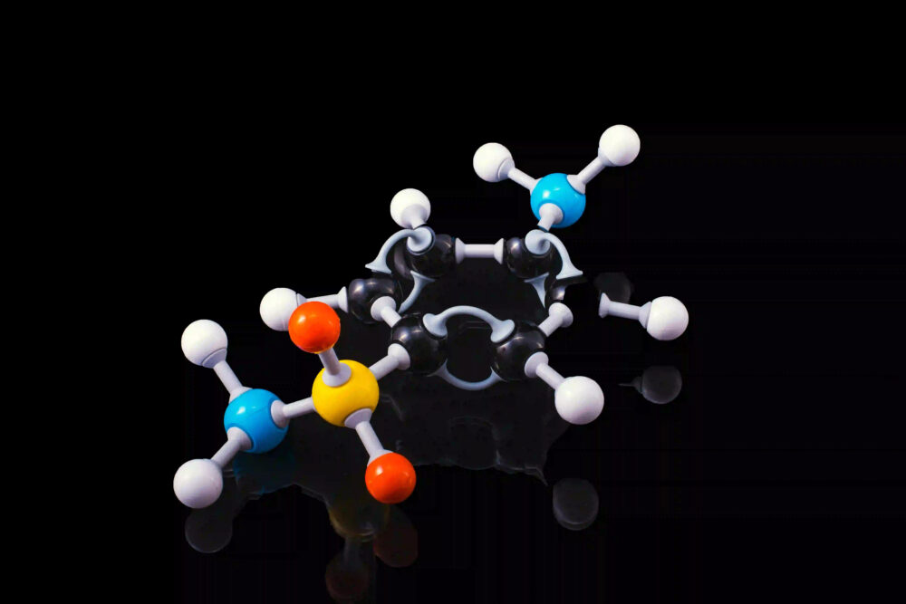
At its core, Chemical Vapor Deposition involves the deposition of thin films onto substrates through the chemical reaction of gaseous precursors. This process occurs within a controlled environment, typically within a vacuum or at elevated temperatures, where precursor molecules dissociate and react on the substrate surface, forming a solid film layer. The choice of precursor materials, reaction conditions, and deposition techniques profoundly influences the properties of the resulting thin film, offering a tailored approach to material synthesis.
Types of Chemical Vapor Deposition
Chemical Vapor Deposition encompasses a spectrum of techniques tailored to specific applications and material requirements. Some prominent variants include:
Metalorganic Chemical Vapor Deposition (MOCVD): Primarily used in semiconductor manufacturing, MOCVD utilizes organometallic precursors to deposit thin films of semiconductor materials like gallium nitride (GaN) and indium phosphide (InP) with high purity and crystalline quality.
Atomic Layer Deposition (ALD): Unlike traditional CVD, ALD relies on sequential, self-limiting surface reactions to achieve precise control over film thickness and conformality, making it ideal for coating complex three-dimensional structures at the atomic level.
Plasma-Enhanced Chemical Vapor Deposition (PECVD): By introducing plasma into the deposition chamber, PECVD enhances the reactivity of precursor gases, enabling the deposition of thin films at lower temperatures and facilitating the incorporation of functional groups for specialized applications such as surface modification and biomaterials synthesis.
Challenges in Thin Film Growth
While Chemical Vapor Deposition offers a versatile platform for thin film fabrication, several challenges persist, limiting its widespread adoption and effectiveness in certain applications.
Precursor Decomposition and Film Contamination
One of the primary challenges in CVD is the controlled decomposition of precursor molecules to deposit pure and uniform thin films. Unintended reactions or impurities can lead to film contamination, altering material properties and compromising device performance. Achieving precise control over precursor chemistry and deposition conditions is crucial to mitigating these challenges and ensuring the reproducibility of thin film growth processes.
Uniformity and Thickness Control
Maintaining uniform film thickness across large-area substrates poses a significant challenge in CVD, particularly for high-throughput manufacturing applications. Variations in precursor flow rates, temperature gradients, and substrate topography can result in non-uniform deposition profiles, leading to inconsistent film properties and device performance. Advanced process monitoring and control strategies, such as real-time spectroscopic techniques and temperature profiling, are essential for achieving uniform thin film growth and enhancing manufacturing yield.
Substrate Compatibility and Film Adhesion
The choice of substrate material and surface preparation significantly influences thin film adhesion and interfacial properties. Mismatched thermal expansion coefficients, surface roughness, or chemical reactivity can compromise film-substrate adhesion and mechanical stability, limiting the reliability and durability of thin film-based devices. Addressing substrate compatibility issues through surface modification techniques and interlayer deposition strategies is critical for enhancing film adhesion and optimizing device performance in diverse operating environments.
Opportunities for Innovation and Advancement
Despite the inherent challenges, Chemical Vapor Deposition continues to evolve as a leading thin film deposition technique, driven by ongoing innovations in materials science, process engineering, and device integration. Several promising opportunities exist for advancing CVD technology and unlocking new avenues for thin film growth and applications.
Novel Precursor Design and Synthesis
The development of novel precursor materials with tailored chemical reactivity and thermal stability holds immense potential for enhancing thin film deposition processes and expanding the range of accessible materials. By leveraging advances in organometallic chemistry and molecular design, researchers can engineer precursors with enhanced volatility, reduced decomposition temperatures, and improved selectivity, enabling the deposition of complex thin film architectures with unprecedented control and precision.
Multi-Scale Process Modeling and Simulation
The integration of multi-scale process modeling and simulation techniques provides valuable insights into the underlying mechanisms governing thin film growth kinetics and substrate interactions in Chemical Vapor Deposition. By coupling computational modeling with experimental data, researchers can optimize deposition parameters, predict film properties, and design customized deposition strategies tailored to specific material systems and device requirements. This synergistic approach accelerates the development of next-generation thin film technologies and facilitates the rapid prototyping of novel materials for emerging applications in electronics, photonics, and energy storage.
Hybrid Deposition Approaches and Advanced Manufacturing
Hybrid deposition approaches, combining CVD with complementary thin film deposition techniques such as physical vapor deposition (PVD) or solution-based methods, offer synergistic advantages for enhancing film quality, scalability, and device integration. By harnessing the complementary strengths of different deposition processes, researchers can overcome inherent limitations and achieve precise control over film composition, morphology, and functionality, paving the way for the development of multifunctional thin film coatings and heterostructures with tailored properties for diverse applications, including optoelectronics, catalysis, and flexible electronics.
Conclusion
Chemical Vapor Deposition stands at the forefront of thin film fabrication, offering unparalleled control over material synthesis and device integration for a wide range of applications. While challenges such as precursor decomposition, film uniformity, and substrate compatibility persist, ongoing innovations in materials science and process engineering present exciting opportunities for advancing CVD technology and unlocking new frontiers in thin film growth and device performance. By addressing these challenges and embracing emerging opportunities for innovation, researchers and engineers can harness the full potential of Chemical Vapor Deposition to drive transformative advancements in materials science, electronics, and beyond.