Chemical Vapor Deposition (CVD) is a widely used technique in materials science and engineering for the synthesis and growth of thin films and coatings. It offers precise control over film properties, such as thickness, composition, and morphology, making it essential for various applications ranging from semiconductor devices to protective coatings. In this blog post, we will delve into the fascinating world of CVD, exploring its growth mechanisms, control parameters, and the diverse range of materials that can be synthesized using this versatile technique.
Understanding the Basics of CVD
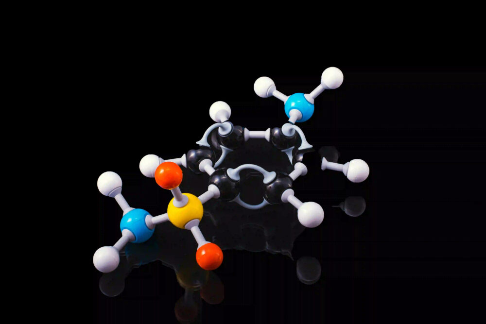
At its core, CVD involves the deposition of a solid material onto a substrate through the chemical reaction of gaseous precursors. The process takes place in a reactor chamber, where the precursors are introduced and react to form the desired material on the substrate surface. The precursors typically consist of volatile compounds containing the desired elements or functional groups. The reaction is initiated by providing energy to the system, which can be achieved through thermal, plasma, or laser activation.
Growth Mechanisms in CVD
Several growth mechanisms govern the deposition of thin films during CVD. The choice of mechanism depends on factors such as temperature, pressure, reactant concentration, and precursor properties. Let’s explore three common growth mechanisms:
Surface Reaction Limited: In this mechanism, the rate of film growth is primarily controlled by the surface reaction between the precursor molecules and the substrate. The availability of reactive sites on the substrate surface plays a crucial role in determining the growth rate. This mechanism often leads to conformal coating with good step coverage.
Mass Transport Limited: Here, the transport of precursor molecules from the gas phase to the substrate surface becomes the limiting factor. Diffusion and convection play significant roles in this mechanism, especially at lower temperatures or higher pressures. Films grown under mass transport limited conditions may exhibit uneven thickness distribution and poor step coverage.
Mixed Control: In certain cases, both surface reaction and mass transport contribute to the growth rate. This mixed control regime occurs when the reaction kinetics and precursor transport are comparable in terms of their impact on film growth. Optimizing the growth conditions becomes crucial to achieve the desired film properties.
Controlling CVD: Key Parameters and Strategies
To achieve precise control over the deposition process and resulting film properties, various parameters need to be considered. Although specific requirements vary depending on the material system, a few key parameters are universally important:
Temperature: Temperature plays a critical role in CVD, influencing the reaction kinetics, precursor adsorption, and film nucleation. Higher temperatures generally enhance deposition rates but can also lead to increased unwanted reactions or decomposition of precursors. Careful optimization is necessary to balance these factors.
Pressure: The pressure inside the reactor chamber affects the gas-phase transport and reaction rates. Higher pressures can promote higher deposition rates but may also result in increased precursor decomposition. Low pressures, on the other hand, may lead to slower growth rates and reduced film quality. Finding the optimal pressure for each specific material system is crucial.
Precursor Concentration: The concentration of precursor gases in the reactor chamber significantly influences the deposition rate and film composition. Higher precursor concentrations typically result in faster growth rates but can also lead to non-uniform film properties or issues like parasitic reactions. Balancing the precursor concentration is key to achieve desired film properties.
Substrate Choice and Preparation: The choice of substrate material and its preparation are vital in CVD. The substrate should have suitable surface properties, such as cleanliness, roughness, and crystallographic orientation, to facilitate nucleation and adhesion of the deposited film. Proper surface treatment, such as cleaning and annealing, is often required before deposition.
Applications and Advancements in CVD
Chemical Vapor Deposition finds applications in a wide range of fields, including microelectronics, optics, energy storage, and biomedical devices. Semiconductor industry heavily relies on CVD for the growth of high-quality epitaxial layers and thin films used in integrated circuits. CVD is also extensively used for the deposition of protective coatings, such as diamond-like carbon (DLC), for enhancing the durability and wear resistance of various materials.
Advancements in CVD techniques continue to expand the repertoire of materials that can be synthesized. For instance, low-pressure CVD (LPCVD) and plasma-enhanced CVD (PECVD) have enabled the growth of complex materials like nitrides, oxides, and carbides. Atomic layer deposition (ALD), a variant of CVD, allows for precise control over film thickness at the atomic level, enabling the fabrication of nanoscale devices.
Conclusion
Chemical Vapor Deposition (CVD) stands as a versatile and powerful technique for the growth of thin films and coatings. By understanding the growth mechanisms and controlling key parameters, researchers can tailor the properties of deposited materials to meet specific application requirements. With ongoing advancements in CVD technology, the range of materials that can be synthesized continues to expand, opening doors to new possibilities in fields such as electronics, optics, and surface engineering. As we delve deeper into the intricacies of CVD, we uncover exciting opportunities for innovation and discovery, driving progress in materials science and engineering.