Chemical Vapor Deposition (CVD) is a versatile technique used in the fabrication of thin films with precise control over thickness, composition, and structure. CVD has become a cornerstone in various industries, including semiconductor manufacturing, aerospace, and optics. In this article, we’ll explore the principles of CVD, its applications, and the different variants of this technique.
Understanding Chemical Vapor Deposition (CVD)
Chemical Vapor Deposition (CVD) is a process used to deposit thin films onto a substrate by introducing volatile precursors into a reaction chamber. These precursors undergo chemical reactions, leading to the formation of a solid thin film on the substrate surface. CVD offers several advantages, including excellent control over film properties, scalability, and the ability to deposit films on complex-shaped substrates.
The CVD Process
The CVD process typically involves several steps:
Preparation of Substrate: The substrate is cleaned and prepared to ensure good adhesion of the thin film.
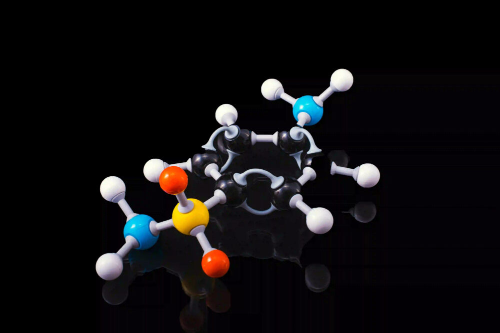
Introduction of Precursors: Volatile precursors are introduced into the reaction chamber either in gas or vapor form. These precursors contain the elements needed for the desired thin film composition.
Chemical Reactions: The precursors undergo chemical reactions, leading to the formation of solid products. These reactions can be thermally or photochemically driven, depending on the CVD variant.
Deposition onto Substrate: The solid products are deposited onto the substrate surface, forming a thin film.
Film Growth and Control: The thin film continues to grow as long as the precursors are supplied. Various parameters, such as temperature, pressure, and precursor flow rates, are controlled to achieve the desired film properties.
Post-Processing: After deposition, the thin film may undergo post-processing steps, such as annealing, to improve its properties.
Types of CVD Techniques
1. Low-Pressure Chemical Vapor Deposition (LPCVD):
LPCVD operates at reduced pressures, typically below atmospheric pressure, to enhance the transport of precursors and improve film quality. It is commonly used in semiconductor manufacturing for depositing silicon dioxide (SiO2) and polysilicon thin films.
2. Atmospheric Pressure Chemical Vapor Deposition (APCVD):
APCVD operates at atmospheric pressure, making it simpler and more cost-effective than LPCVD. However, the film quality may be lower due to reduced control over the deposition process. APCVD is often used for depositing thin films in large-scale applications, such as coatings on architectural glass.
3. Metal-Organic Chemical Vapor Deposition (MOCVD):
MOCVD uses metal-organic precursors, which contain metal atoms bonded to organic ligands. This technique is widely used for depositing compound semiconductors, such as gallium nitride (GaN) and indium phosphide (InP), used in optoelectronic devices.
4. Plasma-Enhanced Chemical Vapor Deposition (PECVD):
PECVD uses plasma to enhance the chemical reactions and improve film quality. Plasma can break down complex precursors into reactive species, leading to lower deposition temperatures and better film properties. PECVD is commonly used for depositing thin films in the microelectronics industry.
Applications of CVD
CVD is used in a wide range of applications, including:
- Semiconductor Manufacturing: CVD is used to deposit thin films in integrated circuits, MEMS devices, and photovoltaic cells.
- Optical Coatings: CVD is used to deposit anti-reflective coatings, reflective coatings, and optical filters on lenses and mirrors.
- Barrier Coatings: CVD is used to deposit thin films for moisture and corrosion protection in packaging materials.
- Decorative Coatings: CVD is used to deposit decorative coatings on glass, ceramics, and metals for aesthetic purposes.
Conclusion
Chemical Vapor Deposition (CVD) is a versatile technique for depositing thin films with precise control over properties. By understanding the principles of CVD and its various variants, researchers and engineers can tailor thin film deposition processes to suit specific applications in industries such as semiconductor manufacturing, optics, and coatings. As technology advances, CVD continues to play a crucial role in enabling the development of innovative products with enhanced performance and functionality.