Chemical Vapor Deposition (CVD) is a versatile and widely used technique for depositing thin films of various materials onto substrates. This process plays a crucial role in the production of a wide range of technological devices, from semiconductor chips to protective coatings. In this blog post, we’ll explore the principles of CVD, its applications, and its importance in modern technology.
The Basics of Chemical Vapor Deposition
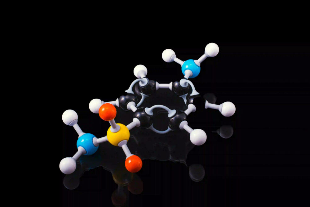
Chemical Vapor Deposition is a process used to deposit thin films of materials onto a substrate by exposing it to one or more volatile precursors, which react and form a solid film on the substrate surface. The precursors are typically gases or vapors that react at the substrate surface or in the gas phase to form the desired material.
Types of CVD
There are several variations of CVD, including:
- Low-Pressure CVD (LPCVD): Operates at reduced pressures, enabling better control over film thickness and properties.
- Atmospheric Pressure CVD (APCVD): Operates at ambient pressure, simplifying equipment requirements but offering less precise control.
- Metalorganic CVD (MOCVD): Uses metalorganic precursors for depositing compound semiconductors and other materials.
The CVD Process
The CVD process typically involves several key steps:
- Precursor Delivery: Volatile precursors are introduced into a reaction chamber containing the substrate.
- Chemical Reaction: The precursors undergo chemical reactions, either at the substrate surface or in the gas phase, forming a solid film.
- Film Deposition: The solid film grows on the substrate surface, with the thickness controlled by the deposition conditions.
- Byproduct Removal: Any byproducts of the reaction are removed from the chamber to prevent contamination.
- Film Annealing (Optional): In some cases, the deposited film may undergo annealing to improve its properties.
Applications of CVD
Chemical Vapor Deposition has a wide range of applications in various industries, including:
- Semiconductor Industry: CVD is used to deposit thin films of silicon dioxide, silicon nitride, and other materials onto semiconductor wafers for integrated circuit fabrication.
- Optical Coatings: CVD is used to deposit anti-reflective coatings, mirrors, and other optical coatings onto lenses and other optical components.
- Hard Coatings: CVD is used to deposit hard, wear-resistant coatings onto cutting tools, bearings, and other components.
- Solar Cells: CVD is used to deposit thin films of semiconductor materials onto substrates for solar cell fabrication.
- Biomedical Applications: CVD is used to deposit biocompatible coatings onto medical implants and devices.
Importance of CVD in Technology
Chemical Vapor Deposition plays a critical role in the development of advanced technologies by enabling the deposition of thin films with precise control over thickness, composition, and properties. This level of control is essential for the fabrication of microelectronic devices, optical components, and other advanced materials used in modern technology.
In conclusion, Chemical Vapor Deposition is a powerful and versatile technique for depositing thin films of materials onto substrates. Its applications span a wide range of industries, and its importance in the development of advanced technologies cannot be overstated. As technology continues to advance, the role of CVD in enabling the fabrication of new and innovative devices will only become more prominent.