Nanotechnology, the science of manipulating matter at the atomic and molecular scale, has garnered significant attention for its potential to revolutionize various fields, from medicine to electronics. In the realm of electronics, nanotechnology holds particular promise, offering the ability to shrink electronic components to the atomic scale. In this blog post, we’ll explore the fascinating world of nanoelectronics and delve into the revolutionary potential of shrinking electronics to the atomic scale.
Understanding Nanoelectronics
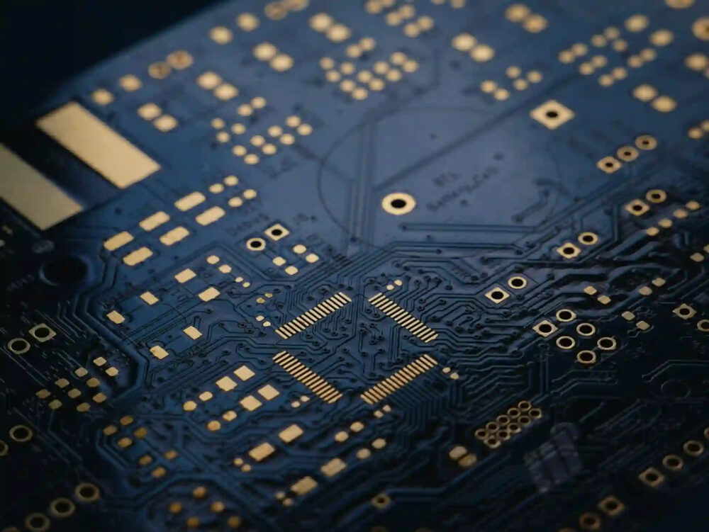
Nanoelectronics refers to the study and application of electronic devices and systems constructed on the nanometer scale. At this scale, materials exhibit unique physical and chemical properties that differ from their bulk counterparts. By harnessing these properties, researchers can develop electronic components with enhanced performance, reduced power consumption, and increased functionality.
The Role of Nanomaterials
Central to the field of nanoelectronics are nanomaterials, which include nanoparticles, nanowires, and two-dimensional materials such as graphene. These materials possess extraordinary electrical, thermal, and mechanical properties due to their nanoscale dimensions. For example, graphene, a single layer of carbon atoms arranged in a hexagonal lattice, exhibits exceptional conductivity and mechanical strength, making it an ideal candidate for next-generation electronic devices.
Advantages of Nanoelectronics
The shift towards nanoelectronics offers several advantages over conventional electronics. By miniaturizing electronic components to the nanoscale, researchers can increase device density, reduce power consumption, and improve performance. Additionally, nanoelectronics enables the development of flexible and transparent electronics, opening up new possibilities for wearable devices, flexible displays, and biomedical implants.
Shrinking Electronics to the Atomic Scale
One of the most exciting frontiers in nanoelectronics is the concept of shrinking electronic components to the atomic scale. This involves manipulating individual atoms to create functional devices with unprecedented precision and efficiency. Several groundbreaking techniques are driving this paradigm shift, including atomic layer deposition, scanning tunneling microscopy, and molecular self-assembly.
Atomic Layer Deposition (ALD)
Atomic layer deposition is a thin-film deposition technique that enables precise control over film thickness at the atomic level. By sequentially exposing a substrate to alternating precursor gases, researchers can deposit uniform layers of material with atomic-scale precision. ALD is widely used in the fabrication of transistors, capacitors, and other semiconductor devices, offering superior control over device dimensions and electrical properties.
Scanning Tunneling Microscopy (STM)
Scanning tunneling microscopy is a powerful imaging technique that allows researchers to visualize and manipulate individual atoms on a surface. By scanning a sharp metal tip across a sample surface, researchers can measure variations in electron tunneling currents, providing atomic-scale resolution. STM has been instrumental in studying the electronic properties of nanomaterials and fabricating atomic-scale structures for nanoelectronic devices.
Molecular Self-Assembly
Molecular self-assembly is a bottom-up approach to nanofabrication, where molecules spontaneously organize themselves into predetermined structures through non-covalent interactions. This technique enables the creation of complex nanostructures with atomic-scale precision, offering a scalable and cost-effective approach to nanoelectronics. Molecular self-assembly holds promise for applications such as nanoscale circuitry, quantum computing, and molecular electronics.
Applications and Future Prospects
The ability to shrink electronics to the atomic scale has profound implications for a wide range of applications. In addition to advancing conventional electronics, nanotechnology enables the development of entirely new classes of devices, such as quantum computers, neuromorphic computing systems, and bioelectronic implants. Furthermore, nanoelectronics holds promise for addressing grand challenges in energy storage, environmental monitoring, and healthcare diagnostics.
Quantum Computing
Quantum computing, which leverages the principles of quantum mechanics to perform calculations at unprecedented speeds, relies on nanoelectronic components such as quantum dots, superconducting qubits, and spintronics devices. By harnessing the unique properties of quantum systems, researchers aim to tackle complex problems in cryptography, material science, and drug discovery that are beyond the reach of classical computers.
Bioelectronic Implants
Bioelectronic implants, such as neural interfaces and biosensors, represent another exciting application of nanoelectronics. By interfacing electronic devices with biological systems at the cellular and molecular level, researchers can develop novel therapies for neurological disorders, monitor physiological parameters in real-time, and enable new modes of human-computer interaction. Nanotechnology enables the fabrication of biocompatible and miniaturized devices that can seamlessly integrate with the human body.
Conclusion: Unlocking the Potential of Nanoelectronics
In conclusion, nanotechnology is poised to revolutionize the field of electronics by shrinking electronic components to the atomic scale. Through advances in nanomaterials, fabrication techniques, and device architectures, researchers are unlocking new opportunities for innovation in areas such as quantum computing, bioelectronics, and beyond. As we continue to explore the potential of nanoelectronics, the future holds immense promise for creating smarter, more efficient, and more sustainable electronic devices that will shape the world of tomorrow.